The word LASER is an acronym: Light Amplification by Stimulated Emission of Radiation. It was coined in 1957 by the physicist Gordon Gould. What distinguishes laser light from LED light is not its colour or its source but three optical properties that come together only in a laser:
- Monochromaticity — the light emerges at one wavelength, often within a fraction of a nanometre. An LED, by comparison, spreads its output across 20 to 40 nm.
- Coherence — every photon emerges in phase with its neighbours, like a marching band stepping in time. Coherence is what allows lasers to be used for high-precision distance measurement.
- Collimation — the beam is narrow and stays narrow. A laser pointer paints a small dot even at fifty metres; an LED at the same drive power would illuminate an entire wall.
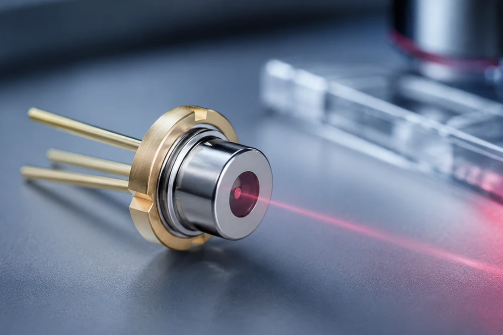
This article focuses on IR lasers and one of their two architectures, the VCSEL (Vertical-Cavity Surface-Emitting Laser).
The Structure of VCSELs
VCSEL was invented in 1977 by Kenichi Iga at the Tokyo Institute of Technology and commercialised in the 1990s. VCSEL has a very complex structure that allows it to behave the way it does.
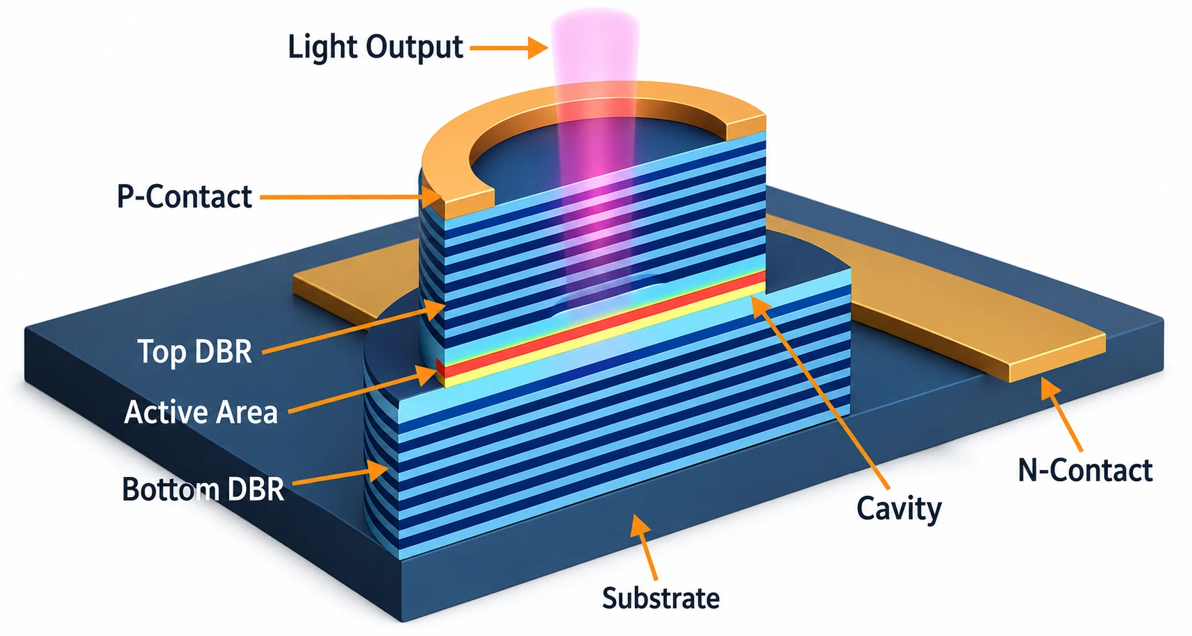
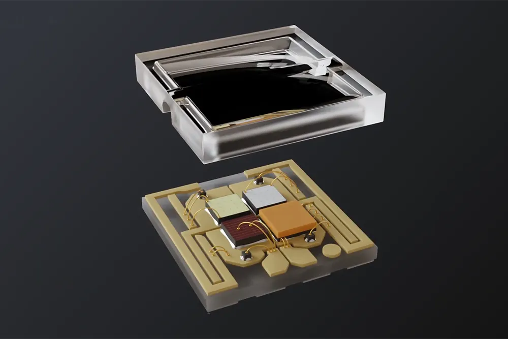
A VCSEL can be explained as a microscopic sandwich of several dozen tiny layers.
The whole structure of layers is grown on a crystal foundation called the substrate, which is usually gallium arsenide. The substrate provides mechanical support; the laser itself is built from semiconductor layers grown on top of it. A pure semiconductor crystal carries very little current on its own, so to make these layers useful, they are "doped" by adding tiny amounts of different elements to the crystal lattice.
The lower, bottom layers are doped with an element whose atoms have extra electrons, which leaves free electrons to wander through the crystal. Because electrons carry negative charge, this region is called n-type, where n stands for negative.
The upper, top layers are doped with an element that is short one electron, which leaves the bonding structure with missing electrons — so-called holes — that move through the crystal as if they were positive charges, making this region called p-type, where p stands for positive.
At the top and the bottom of that sandwich sit two special mirrors — n-DBR (n-Distributed Bragg Reflector) at the bottom and p-DBR (p-Distributed Bragg Reflector) at the top. Both reflect more than 99% of the light. The bottom mirror is typically slightly more reflective at around 99.9%, while the top one is around 99.5% — the small difference is deliberate, since the laser beam needs to exit through the top.
The space between the mirrors is called the cavity — a small chamber tuned so that exactly one wavelength of light fits inside, and that is the wavelength the laser emits. The cavity contains the active layer where light is produced. When voltage is applied between the p-contact on top and the n-contact at the bottom, electrons stream up from the n-side and holes stream down from the p-side, meeting exactly in the active layer and recombining to release light.
A special process leaves a narrow conductive channel through the middle of one nearby layer, while everything around it is turned into an insulator. This forces the current to flow only through the centre, exactly where the light is born. The particles of light born there bounce up and down between the two mirrors until there are so many of them that some leak straight upward through a central hole in the metal ring on top. Together they form a thin laser beam.
The 2017 launch of Apple's Face ID in iPhone X brought the VCSEL into the consumer mainstream: a near-infrared VCSEL array behind a DOE (Diffractive Optical Element) projects 30,000 invisible dots onto the user's face, a separate VCSEL plus sensor measures depth by time-of-flight, and the phone reconstructs a 3D model of the face from the result.
What Does Sensing Technology Actually Do — and Why It Needs a Laser
Two VCSEL-based measurement techniques drive the majority of today's industrial VCSEL demand:
- Time-of-Flight (ToF) ranging
- Structured light
Each uses VCSELs in a different way, and the technical mechanism behind each is worth understanding in detail. These measurements provide the input for the interpretation of results in 3D Vision.
Time-of-Flight
ToF measures distance by timing how long it takes for light to leave the laser, reach a target, and reflect back. There are two types of ToF systems — direct and indirect.
- Direct ToF (dToF) — the VCSEL emits a short pulse. The pulse travels to the target, reflects, and a small fraction returns to the detector called SPAD (Single Photon Avalanche Diode), which timestamps each returning photon with very high precision. A circuit called TDC (Time-to-Digital Converter) measures the time between emission and arrival.
- Indirect ToF (iToF) — instead of a short pulse, a continuous wave is emitted. The reflected light arrives at the detector with a phase shift relative to the emitted wave, because it had to travel out and back. By sampling the returned light at several phase windows (usually four, at 0°, 90°, 180°, and 270°), the system calculates the phase shift and from it the distance.
Structured Light
Where ToF measures distance through time, structured light measures distance through space — by reading how a projected pattern deforms across the scene.
Structured light projects a pattern of light onto a scene and reads the scene's 3D shape from how that pattern deforms across the target's surface. Imagine projecting a grid of dots onto a flat wall — every dot appears exactly where you expect it. Now imagine projecting the same grid onto a face. The dots wrap around the curves, bunching where the surface is closer to the projector and spreading where it is farther. An IR camera positioned alongside the projector can measure these shifts and, with the right geometry, reconstruct the 3D shape of the face.
The light source is a VCSEL placed behind a DOE (Diffractive Optical Element) — a small piece of glass or polymer with a precisely etched microscopic surface pattern. When the VCSEL beam passes through it, diffraction splits the single beam into thousands of distinct beamlets, each emerging at a slightly different angle. Together they create the projected dot field.
The dot pattern itself is not random. It is designed so that any small group of dots, anywhere in the field of view, is locally unique. This uniqueness allows the system's software to match each dot it sees in the camera image to its expected position in the projected pattern. The displacement between expected and observed position — known as disparity — translates directly into depth, through simple geometric triangulation between the emitter, the camera, and the surface point.
3D Vision
A sensor like ToF or structured light measures the world. 3D Vision interprets what those measurements mean. The sensor outputs a long list of depth values — just numbers. 3D Vision is software that reads those numbers and turns them into something the machine can act on: "A person just stepped two metres ahead." "This part is rotated 23 degrees." "The bottle has a dent on its left side." Without 3D Vision, the sensor is only measuring. With 3D Vision, the system is seeing and acting.
What VCSELs change is how easy it has become to build the sensor side for short- and medium-range 3D systems. In the past, getting good 3D data at this range usually required bulky mechanical scanners. VCSEL arrays opened a more compact alternative.
VCSEL Portfolio
Edison Opto manufactures two distinct VCSEL families, each targeting a different range of applications.
High-Power VCSEL Portfolio
The high-power family drives ToF and structured light systems where output power and pulse fidelity matter most. The three parts in this family are optimised for short, high-current pulses rather than continuous operation. Brief duty cycles allow modest average-power devices to deliver large bursts of peak optical power for the few nanoseconds of a ranging pulse.
| Model | Package (mm) | Drive Current (mA) | Radiant Power (mW) | Voltage (V) | Primary Use |
|---|---|---|---|---|---|
| EDVCSEL-IC | 3.5 × 3.2 × 1.45 | 1250 / 2750 pulse | 1100 – 2800 | 1.9 – 2.1 | ToF emitter |
| EDVCSEL-BH | 3.5 × 3.5 × 3.98 | 1000 / 1500 pulse | 630 – 930 | 1.9 – 2.1 | Structured light |
| EDVCSEL-FC | 3.5 × 3.5 × 2.3 | 2750 pulse | 2400 | 1.9 – 2.1 | Moulded lens |
EDVCSEL-IC is the ToF workhorse — the flattest of the three at just 1.45 mm tall, delivering up to 2.8 W of pulsed radiant power. Specify this part when the receiving side is a SPAD detector plus a timing chain.
EDVCSEL-BH is taller because it carries an integrated diffractive optical element (DOE). The DOE splits the VCSEL output into a dense array of dots projected across the scene — the part for structured light 3D scanning, where the receiving side is a camera reading dot positions. Available in three configurations: 62°×64° (11,232 dots), 80°×60° (10,980 dots), and 93°×70° (15,372 dots).
EDVCSEL-FC uses a moulded lens for use where a controlled beam pattern matters more than maximum range.
Low-Power VCSEL Portfolio
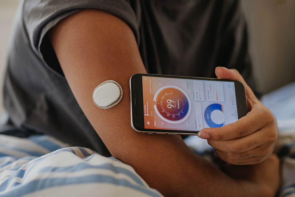
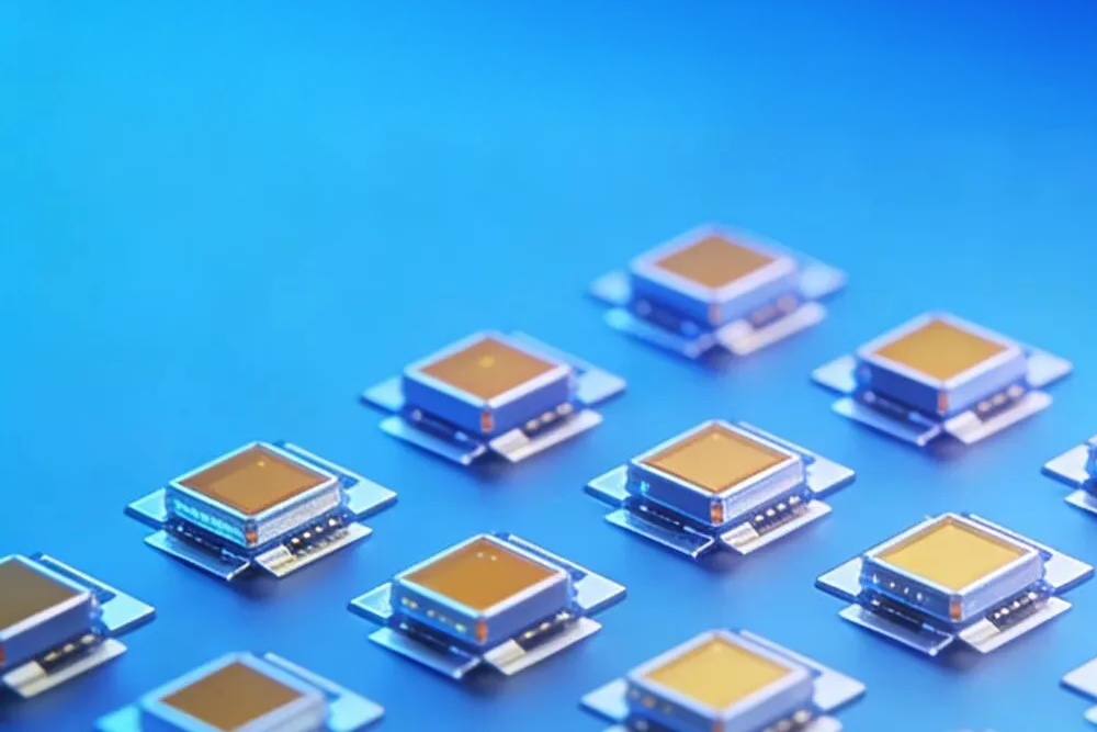
Not every laser application asks for watts of peak power. A smartwatch reading heart-rate variability through the skin, a fingerprint sensor under a glass cover, a hand-held beauty device delivering low-level light therapy to the dermis — all of these need a small, low-current laser source, often at a wavelength specifically chosen for what the tissue does with the photons. The low-power family targets wearables, biometric sensing, and consumer health devices where size and current draw are the real constraint.
| Model | Package (mm) | Chip Wavelength (nm) | Chip Optical Power (mW) | Chip Voltage (V) | Operating Current (mA) |
|---|---|---|---|---|---|
| RTSA0117SD252507 | 3.0 × 1.4 × 0.7 | 660 | 3 | 2.5 | 9 |
| RTST0120S720200B | 3.0 × 1.4 × 0.7 | 940 | 14 | 1.8 | 10 |
| RTHS15M1X1303007 | 3.4 × 3.3 × 1.9 | 680 / 850 / 940 | 3 – 7 | 2.1 – 2.5 | 12 / 9 |
Edison's low-power VCSEL family covers exactly this niche. The package is plastic and tiny — 3 × 1.4 × 0.7 mm for the smallest parts. Operating currents are in the 9 to 12 mA range; optical powers from 3 to 14 mW. Multiple wavelengths are offered to match the biological target.
The 660 nm RTSA is a visible red VCSEL useful for biometric sensing where the wavelength is chosen to interact with haemoglobin and skin pigmentation in a controlled way.
The 940 nm RTST sits at the deep-near-infrared end — invisible to the eye, with strong tissue penetration; it is the same band used for pulse oximetry on the wrist.
The RTHS is the small-format structured-light cousin of the high-power EDVCSEL-BH — a multi-wavelength VCSEL for applications requiring multiple sensing bands in one package.
Where Telcona Fits
Telcona's role is to bring Edison Opto's optical portfolio into the European sensor industry, together with the engineering support customers need to use it well. Edison Opto's catalogue spans the full optoelectronic stack: indication LEDs, photoelectric and ToF emitters, high-power VCSELs for ToF and structured light, low-power VCSELs for wearables and biometrics, edge-emitting lasers for medical and industrial applications, photo-interrupters, optical encoders, photodiodes, and complete dToF ranging modules.
Beyond the parts themselves, Edison's LDMS (Lighting Design Manufacturing Service) lets Telcona offer customers more than just components — opening the door to co-engineered subassemblies: custom optics, tailored wavelengths, integrated VCSEL-plus-DOE modules, complete sensor front ends. This matters when a sensor programme needs more than a part number — when the design problem is "help us build the optical engine for our next-generation 3D camera" rather than "find me a 940 nm VCSEL". That kind of work is a meaningful step up from catalogue distribution, and it is where Telcona and Edison together earn their place on a customer's BOM.
Forty years of focus on bridging Asian component manufacturing with European engineering and supply-chain accountability is what Telcona brings to every project: price discipline from established Asian partnerships, quality control from regular factory audits, technical support from Telcona's own engineering team in Belgrade, and a single European contract instead of a tangle of overseas relationships.
👉 For component selection support, free samples, custom optics, integrated ToF or structured-light modules, eye-safety guidance, or a full BOM analysis for your next laser-based sensor programme, contact Telcona — your partner from concept through series production.